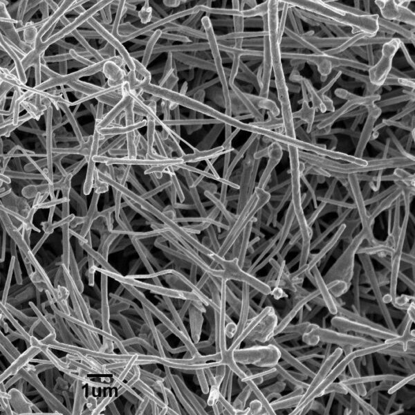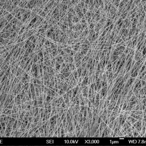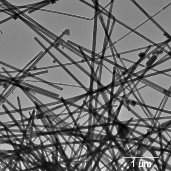

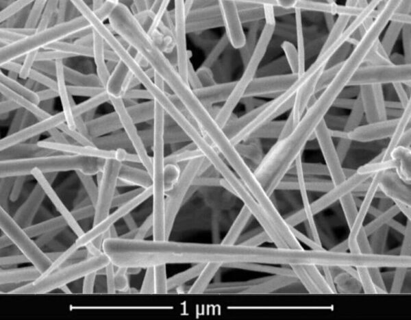
The Copper Nanowires A2 (100nm×10µm) are high-aspect-ratio copper nanomaterials engineered to form efficient conductive networks in electronic, energy, and composite systems. With an average diameter of ~100 nm and a length of ~10 µm, their elongated geometry promotes wire-to-wire contact and creates continuous pathways for electrical and thermal transport. This network-forming capability makes them particularly useful for lightweight, flexible, and three-dimensional conductive structures. Their combination of nanoscale diameter, extended length, and high copper conductivity makes them exceptionally well suited for thin films, flexible electronics, conductive coatings, polymer and ceramic composites, paints, adhesives, and other advanced functional materials.
Catalog Number: NovaWire-Cu-A2-RD
Diameter: ~100 nm
Length: ~10 µm
Appearance: dispersed red suspension
Dispersion solvent: water, ETH, or IPA
Concentration: 10mg/ml
KEY FEATURES
Designed for conductive-network formation, the Copper Nanowires A2 combine high aspect ratio, strong electrical transport, and broad compatibility with advanced material systems.
- Efficient network formation: The elongated wire structure promotes contact between nanowires and supports continuous conductive pathways.
- High electrical and thermal conductivity: Copper enables effective charge and heat transport in films, coatings, and composites.
- High-aspect-ratio geometry: The ~10 µm length helps form interconnected networks while maintaining a nanoscale diameter.
- Flexible material integration: Suitable for incorporation into compatible polymers, ceramics, coatings, paints, adhesives, and composite matrices.
- Broad processing potential: Suitable for coating, printing, mixing, and composite-processing workflows.
APPLICATIONS
The Copper Nanowires A2 provide a versatile conductive material for applications including:
- Flexible and transparent conductive films
- Touchscreens, touch sensors, and flexible displays
- OLEDs, E-paper, smart windows, and solar cells
- Battery, fuel-cell, and supercapacitor components
- Conductive polymer and ceramic composites
- ESD-protection materials
- EMI-shielding gaskets and compositesConductive paints, coatings, adhesives, and inks
REFERENCES
- Nobuya Tanaka, Shinichiro Sonoda, “Conductive Film”, U.S. Patent Application Publication, 2024, No. US 2024/0004505 A1, published January 4, 2024.
SYNONYM
Cu nanowires, copper nanofibers, metallic nanowires, metallic nanofibers, conductive nanowires, conductive nanofibers
RELATED NANOWIRE MATERIALS
Explore other metallic nanowires for conductive material development: