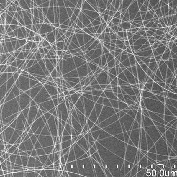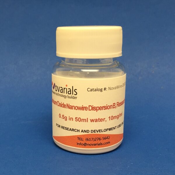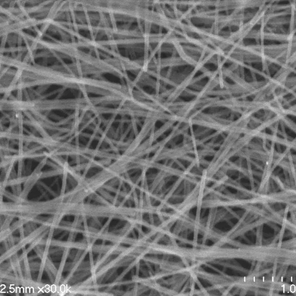

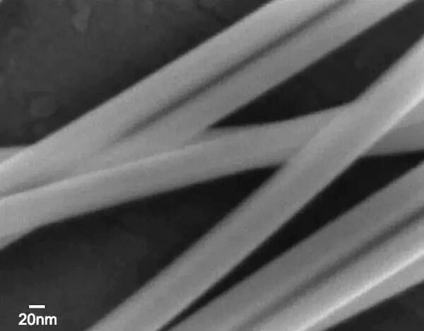
The Silver Nanowires A60 (60nm×45µm) feature a high aspect ratio engineered for applications that demand mechanical durability and stable electrical pathways across large surface areas. With an average diameter of ~60nm and an average length of ~45 µm, these nanowires are particularly well suited for forming robust percolation networks in conductive films and large-area conductive coatings. They can be used in transparent electrodes, flexible electronics, touch sensors, conductive films, printed conductive networks, EMI shielding coatings, strain sensors, and other advanced conductive coating applications.
Catalog Number: NovaWire-Ag-A60
Average Diameter: ~60nm
Average Length: ~45µm
Appearance: gray suspension (dispersed in solvent)
Dispersion solvent: water, ETH, IPA, or customized
Concentration: 5mg/ml, 10mg/ml, 20mg/ml, or customized
APPLICATIONS
The Silver Nanowires A60 can be used in the following applications:
- Transparent Conductive Films: Used as alternatives to indium tin oxide (ITO) in touch panels, displays, solar cells, LEDs, OLED devices, and other optoelectronic systems.
- Flexible Electronics: Integrated into bendable and stretchable substrates for flexible displays, antennas, wearable devices, and deformation-tolerant circuits.
- Printed Electronics: Formulated into inks for inkjet and screen printing, enabling scalable fabrication of conductive patterns and components.
- Flexible Transparent Heaters: Applied in defrosting systems, de-icing surfaces, and smart-window technologies.
- Catalysis: Utilized in chemical reactions, including oxidation, reduction, and pollutant degradation.
- Sensors: Incorporated into chemical and gas sensors (e.g., NH₃, NO₂, CO) as well as pressure and strain sensors based on resistance changes.
- Additional applications: liquid crystal displays, e-paper, conductive adhesive fillers, surface-enhanced spectroscopy (SERS), EMI-shielding films and paints, optical limiters, waveguides, and compact logic devices.
SDS
RELATED NANOWIRE MATERIALS
Explore other metallic nanowires for conductive material development: